IMPORTANT: You should consider setting all settings for each chip before constructing your circuit. Changes to settings will require you to check each marked CAM (Marked with a yellow "?") that has already been placed in that chip (see Configuring CAMs).
OkikaVortex and SonicMaster chips
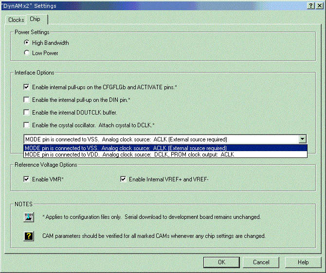
Power Settings
The AnadigmDesigner®2 software also allows chips to operate in a Low Power mode. In this mode all the CAMs are biased for low power operation. Default operation is to use full power, thus achieving higher bandwidths.
The Low Power mode is currently being characterized to determine the effect of lower biasing on the bandwidth and performance of each CAM. Until then, users of the low power mode are advised to verify their designs on the bench.
See Power Management for more details on power issues.
Interface Options
The CFGFLGb & ACTIVATE check box, when checked, activates a weak internal pull-up resistor on each of these pins. (In a multiple DynAMx circuit, this should be done only for the DynAMx with the lowest load order.)
The DIN pin is the serial data input pin. Checking this box activates a weak internal pull-up resistor on this pin. This option should normally be chosen for PROM based designs. (In a multiple DynAMx circuit, this should be done only for the DynAMx with the lowest load order.)
The DOUTCLK buffer is used to buffer the DCLK pin in designs using an external crystal.
The crystal oscillator should be enabled for PROM based designs which use an external crystal rather than an external buffered oscillator.
Mode Pin Settings
If connected to VDD - The DynAMx accepts a free-running clock on the DCLK pin and creates a configuration clock at 1/16th of the DCLK frequency on the ACLK pin. This mode should be chosen only if you are doing a PROM based design. (In a multiple DynAMx circuit, this should be done only for the DynAMx with the lowest load order.)
If connected to VSS - Should be used in all other cases.
Reference Voltage Options
VMR is the analog ground for the DynAMx. In a multiple DynAMx circuit, this should be enabled for the DynAMx with the lowest load order and all VMR pins should be connected together.
VREF+ and VREF- are internal reference voltage sources. In a multiple DynAMx circuit, these should be enabled for the DynAMx with the lowest load order. All VREF+ pins should be connected together. All VREF- pins should be connected together.
OkikaApex
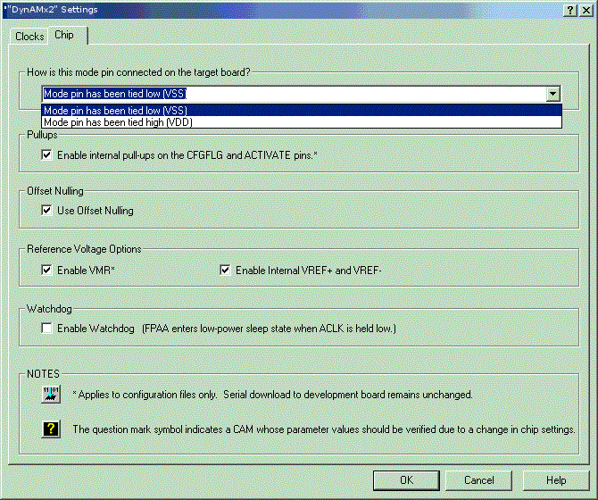
How is the mode pin connected on the target board?
Mode pin has been tied low (VSS) - Should be used in most cases. (See OkikaApex User Manual.)
Mode pin has been tied High (VDD) - The DynAMx accepts a free-running clock on the ACLK pin and creates a configuration clock at 1/16th of the ACLK frequency on the SCLK pin. This is normally appropriate for the DynAMx that drives the PROM clock. (See OkikaApex User manual)
Pullups
The CFGFLGb & ACTIVATE check box, when checked, activates a weak internal pull-up resistor on each of these pins. (In a multiple DynAMx circuit, this should be done only for the DynAMx with the lowest load order.)
Offset Nulling
Offset nulling will cause the DynAMx to run an algorithm at startup time which will attempt to reduce voltage offsets.
Reference Voltage Options
VMR is the analog ground for the DynAMx. In a multiple DynAMx circuit, this should be enabled for the DynAMx with the lowest load order and all VMR pins should be connected together.
VREF+ and VREF- are internal reference voltage sources. In a multiple DynAMx circuit, these should be enabled for the DynAMx with the lowest load order. All VREF+ pins should be connected together. All VREF- pins should be connected together.
Watchdog
If enabled, the DynAMx will enter a sleep state when ACLK stops. When ACLK is restarted, the DynAMx will resume normal operation.