Differential versus Single-Ended
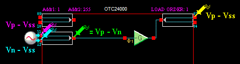
It is important to understand the way that signals are represented in AnadigmDesigner®2. As detailed below, voltages on pins outside the red chip boundary are represented as single-ended signals and voltages on pins inside the red chip boundary (within the DynAMx) are represented as differential values.
All analog signal paths within the DynAMx (inside the red chip boundary) are differential, so AnadigmDesigner®2 represents each differential pair as a single wire. This simplification allows for cleaner schematics and simplified wiring within the DynAmx. A single line represents a differential pair and connections to the differential input or output of CAMs may be represented by a single contact. The simulator in AnadigmDesigner®2 represents voltages internal to the DynAMx as differential values (Vp-Vn). The common mode component of the signals within the chip is not represented in the simulator.
Signals external to the DynAMx (outside the red chip boundary) are represented in AnadigmDesigner®2 as single-ended, earth ground (Vss) referenced signals. The positive and negative components of differential signals are independently represented as (Vp-Vss) and (Vn-Vss), respectively, so that they may be viewed on the virtual oscilloscope just as they would normally be measured with a real oscilloscope on the bench. This allows signals outside the chip to be represented as they would normally be seen with standard test equipment.
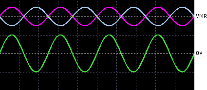
Note that the single-ended representation for input pins on the outside of the array means that it is necessary to include a DC bias in the signal definition so that input signals will vary around the analog signal reference (VMR). This bias is available as a "DC offset" parameter in single-ended signal generators and as the "Common Mode Offset" in differential signal generators.
Also note that all analog DynAMx outputs are differential. Each pin of a differential output cell will deliver half of the differential signal, (Vp-Vn)/2, with the signal on the negative pin inverted with respect to the positive pin. Each of these signals will be biased at a DC voltage equal to VMR. Digital inputs and outputs conform to standard CMOS logic levels (Vdd to Vss).